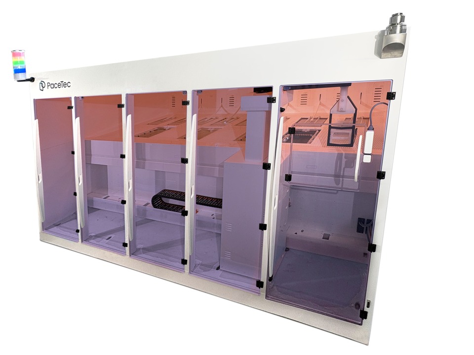
PaceTec successfully delivered a complex high-end project for a leading European semiconductor research institute: the design, manufacturing, and installation of 10 custom-built wet benches (wet process systems) for 200 mm (8-inch) wafer processing in ultra-cleanroom environments.
The project focused on a complete semiconductor wet processing solution for research and development, designed for maximum process stability, reproducibility, and ultra-low particle contamination.

Integrated Wet Process Solution for Semiconductor R&D
The installed wet bench systems cover a wide range of critical semiconductor wet processes:
- HF, BOE, and oxide etching processes
- SC1 and SC2 cleaning with megasonic enhancement
- TMAH-based photoresist development processes
- Posistrip and resist stripping applications
- Ultrasonic acetone and IPA cleaning processes
- Metal etching for advanced microfabrication
Each system is optimized for 8-inch wafer process development lines (PDL) and advanced semiconductor research laboratories.
Ultra-High Purity Design for Semiconductor Manufacturing
A key success factor of this project is its strict Ultra High Purity (UHP) engineering standard:
- Semiconductor-grade materials such as PFA, PTFE, PVDF, and quartz glass
- Fully metal-free wetted surfaces to eliminate contamination risks
- Optimized overflow and laminar flow design for particle reduction
- Validated performance: < 20 particles > 0.3 µm per test wafer
- Ultra-low metal contamination: < 1E10 atoms/cm²
These specifications make the systems ideal for advanced semiconductor processing, MEMS fabrication, and nanotechnology research.

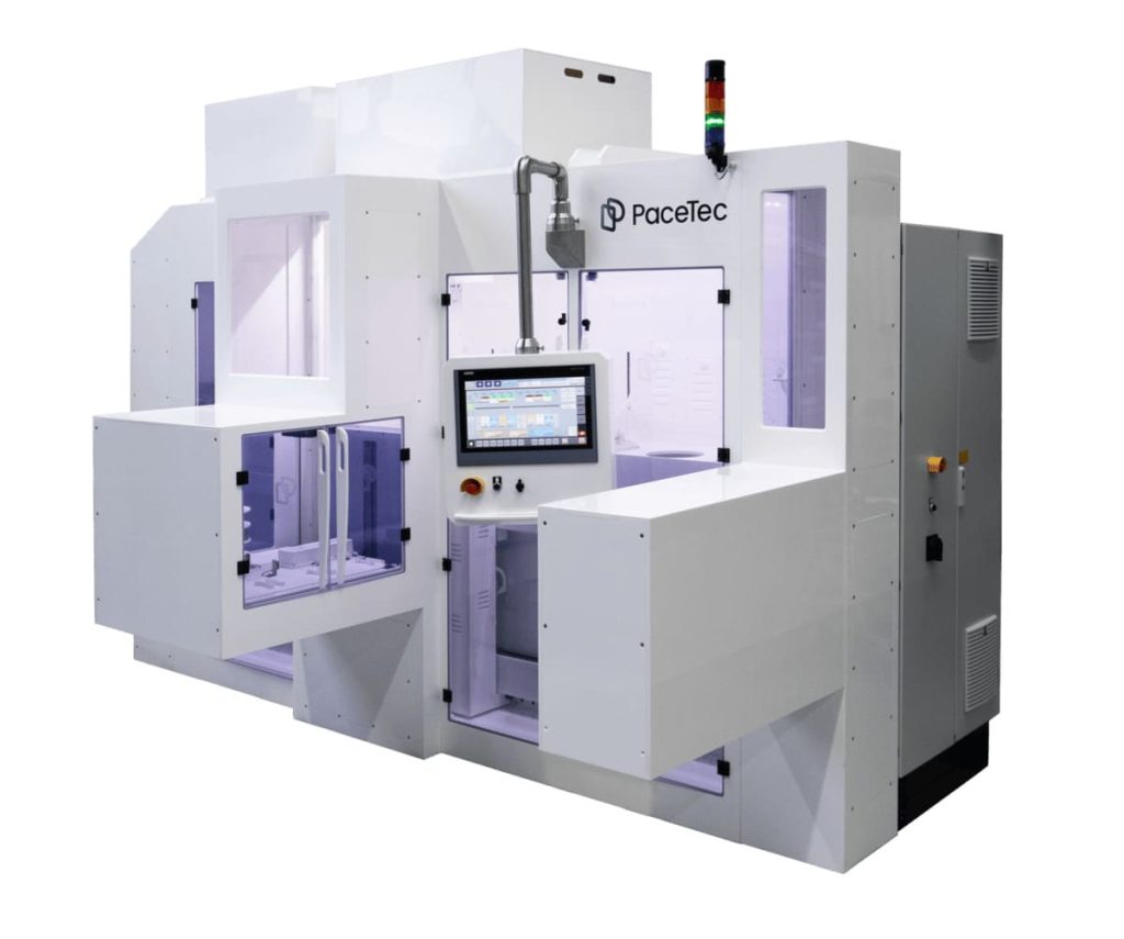
Intelligent Wet Bench Architecture for Maximum Process Control
The systems are engineered for maximum operational safety and precision:
- PID-controlled temperature regulation (±1 °C stability)
- Separated chemical, electrical, and pneumatic chambers with nitrogen purging
- Laminar airflow design for cleanroom compliance
- Integrated leak and spill management via plenum system
- Energy-efficient operation with Active/Idle mode and exhaust reduction
Seamless Integration into Semiconductor Fabs and Research Facilities
The wet benches are fully compatible with modern cleanroom infrastructures:
- DI and hot DI water systems (18 MΩ·cm)
- Chemical supply for SC1, SC2, HF, H₂O₂, NH₄OH, IPA, acetone
- Dedicated drain systems: neutralization, HF, solvents, Posistrip
- Industry-standard interfaces: PFA, Swagelok, VCR fittings
This enables seamless integration into semiconductor fabs, pilot lines, and R&D environments.
Benchmark for Semiconductor Wet Processing Technology
With this project, PaceTec strengthens its position in:
- Semiconductor wet bench systems
- High-purity wet chemical processing equipment
- 8-inch wafer wet processing solutions
- Custom-built R&D semiconductor tools
A reference project setting new standards in wet process technology for advanced semiconductor manufacturing and research.